|
(Zinc Oxide, Zinc Sulfide)
Abstract:
Zinc Oxide and Zinc Sulfide nanostructures were grown on a variety of substrates using aqueous growth solutions. The chemical composition of the nanostructures was characterized using micro-Raman spectroscopy, energy-dispersive X-Ray spectroscopy, and X-Ray diffraction. A Scanning Electron Microscope reveals a well-aligned, uniform, layer of hexagonally shaped Zinc Oxide nanorods growing up perpendicular to the substrate surface while the Zinc Sulfide formed irregularly shaped spheres on the substrate. Depending on the growth conditions, the diameters of the ZnO nanorods ranged from a few hundred nanometers to about 1 μm. The field emission properties of the ZnO nanorods and the ZnS spheroids were studied, with turn-on voltages found to be around 36 v / μm, as well as the effects on ZnS after exposure to various gases which was found to increase the turn-on voltage in most cases.
* Presented at the Texas regional meeting of the American Physical Society (APS), Oct. 2007.
ZnO Introduction
Zinc Oxide nanorods were grown using the method developed by L. Vayssieres [1] using aqueous solutions of a Zinc salt and Hexamine.
-
Zinc Salts Tested:
- Zinc Nitrate, Zn(NO3)2
- Zinc Sulfate, ZnSO4
- Zinc Chloride, ZnCl2
- Zinc Acetate, Zn(C2H3O2)2
-
Substrates Tested:
- Silicon (wafer), Si
- Silver-coated-Silicon, Ag-Si
- Copper-coated-Silicon, Cu-Si
- Nickel-coated-Silicon, Ni-Si
- Aluminum-coated-Silicon, Al-Si
- Brass-coated-Copper (polished / unpolished), Brass-Cu
- Glass (Microscope slide), glass
Metallic coatings on a polished Silicon wafer substrate were deposited by metal evaporation to a usual thickness of 1000 Ǻ (100 nm).
|
|||||||
|
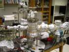
Sample holders were constructed out of small, autoclavable, glass vials. Each vial was filled with growth solution made from the desired Zinc salt and contained one or more substrates of a particular type which were mounted upright within the vial. Once the vials were sealed, they were submerged in a warm water bath (maintained by a programmable hotplate) in order to regulate the temperature during the growth process.
Typically a water bath temperature of around 70 °C for a period of about 3 hours was used to grow the Zinc Oxide nanorods; however the growth temperature, time, solution concentration, and pH may be adjusted so as to grow the nanorods' as desired.
After the allotted growth time, the samples were removed from their vials, rinsed with deionized water, and allowed to air-dry.
Very large ZnO structure may sometimes be visible under an optical microscope if the nanorods are grown under the proper conditions, but a Scanning Electron Microscope (SEM) is often needed in order to resolve the small nanorods which have widths on the order of a few hundred nanometers or smaller.
Pictures taken with an Environmental SEM (ESEM) and High-Resolution SEM are shown below.
Scanning Electron Microscope Images
ESEM Images of Zinc Oxide Nanorods:
|
|||||||||||||||||||
|
High-Resolution SEM Images of Zinc Oxide Nanorods:
|
||||||||
|
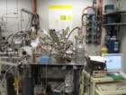
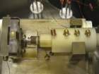
The Field Emitting properties of the ZnO nanorod samples were tested in an Ultra-High Vacuum (UHV) chamber. Higher-than-expected turn-on voltages were measured for the ZnO nanorods (around 36 volts per micrometer), and it is theorized that this is due to the very densely packed and thick nature of the nanorods samples used in the tests. One might expect low turn-on voltages for ZnO nanorods due to their (needle-like) geometry which would concentrate the electric field at the tips of the rods and be more prone to support field emission. However, due to the density of nanorod distribution on the substrate surface as well as the thick nature of rods tested, the sample may have acted almost as a flat plate with no sharp points which would allow the concentration of electric field lines and thus require the application of a higher potential difference before the material field emits. Perhaps with a less-densely packed substrate surfaces and rods with higher aspect ratios, the turn-on voltage would decrease. Such surfaces could, in theory, be grown using the same procedure described above (using aqueous growth solutions), under the right conditions.
ZnS Introduction
An attempt was made to grown Zinc Sulfide nanostructures using the method described by D. A. Johnston, et al, using an aqueous Zinc salt growth solution [2].
Aqueous solutions of Zinc Sulfate (ZnSO4), Thiourea (CH4N2S), and Sodium Citrate (Na3C6H5O7) were used to prepare the growth solution. The growth procedure is very similar to that of the Zinc Oxide nanorods, as described above.
Unfortunately, we did not have nearly as much success in growing Zinc Sulfide nanostructures as we did with Zinc Oxide. Instead of ZnS crystals, irregular blobs grew on the substrate surface with little to no crystal structure visible using an ESEM. Using a High-Resolution Scanning Electron Microscope, these irregular blobs appear to possess a surface structure which resembles balls of yarn. As interesting as this morphology may be, very little Zinc Sulfide was detected on the sample using both energy-dispersive X-Ray spectroscopy (EDAX) and X-Ray diffraction (XRD) to characterize the chemical composition. Most of the material observed seemed to be Zinc Oxide, with only traces of Sulfur detected.
Scanning Electron Microscope Images
SEM Images of Zinc Sulfide:
|
|||||||||
|
Despite the apparent failure to grow Zinc Sulfide on the substrate, the samples field emitting properties were measure to find the effects of exposure to various gasses to the turn-on voltage. It was found that Ar, CO2, O2, and water vapor degraded the field emitting ability of the ZnS sample while N2 showed a slight improvement. H2 initially improved the field emitting ability of the sample but then caused degradation upon longer exposure.
Conclusion
Using an aqueous chemical growth procedure, well-aligned, uniform, layers of Zinc Oxide nanorods were successfully grown on various substrate surfaces. These Zinc Oxide nanorods were found to field emit with a measured turn-on voltage corresponding to about 36 volts per micrometer.
Attempts at growing Zinc Sulfide from aqueous solution produced irregular spherical-shaped structures which were found to be made up of mostly Zinc Oxide with only small, barely detectable, amounts of Zinc Sulfide. The effects of exposure to various gases (Ar, N2, H2, O2, CO2, H2O) on the field emitting properties of the ZnO-ZnS spheroids was measured showing an increase in the turn-on voltages in all cases except Nitrogen gas which showed a slight decrease in the turn on voltage.
For a more detailed description of the growth procedure, chemical characterization of the ZnO / ZnS samples, and field emission results, consult the Poster (.PDF format, 1 MB).
References:
[1] L. Vayssieres, Adv. Mater. 2003, 15, 464.
[2] D. A. Johnston, M. H. Carletto, K. T. R. Reddy, I. Forbes, R. W. Miles,
Thin Solid Films 2002, 403 – 404, 102.
Last updated:
12/19/2007


